简介
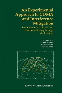
An Experimental Approach to CDMA and Interference Mitigation was written with the admittedly ambitious intent of filling the gap between communication theory and VLSI implementation, and thus to provide a more general/theoretical approach to the design, development, and testing of a CDMA receiver. As a consequence, the concepts and techniques that are presented turn out to be applicable to a more general kind of digital wireless modems in terms of receiver architecture design and implementation. As the reader will easily find out, the subject of digital modem design and implementation is addressed in the book starting from a theoretical approach (supported by proper bibliographic references), and is followed by application issues, with reference to an ESA experiment assumed as a case study. A complete design flow, from specification to implementation, including testing and final verification is then presented. This leads the reader step-by-step to a thorough understanding of CDMA transmission and detection, and constitutes a practical guidance for the design of VLSI wireless mobile terminals.
目录
Contents
Authors
Acknowledgments
Foreword
CHAPTER 1 Introducing Wireless Communications
1. The Wireless Revolution
2. 2G and 3G Wireless Communication Systems in Europe and the USA
3. The role of Satellites in 3G Systems
4. VLSI Technologies for Wireless Communication Terminals
CHAPTER 2 Basics of CDMA for Wireless Communications
1. Narrowband and Wideband Digital Modulations
2. Properties of Spread Spectrum Signals
3. Code Division Multiplexing and Multiple Access
4. Multi-Cell or Multi-Beam CDMA
5. Interference Mitigation Receivers for the Downlink
6. A Sample CDMA Communication System: Specifications of the MUSIC Testbed
CHAPTER 3 Design of an All Digital CDMA Receiver
1. CDMA Receiver Front End
1.1 Multi-Rate CDMA Signal
1.2 Receiver Overall Architecture
1.3 From Analog IF to Digital Baseband
1.4 Decimation and Chip Matched Filtering
2. CDMA Receiver Synchronization
2.1 Timing Synchronization
2.2 Interpolation
2.3 Carrier Synchronization
3. Signal Detection and Interference Mitigation
3.1 EC-BAID Architecture
3.2 EC-BAID Optimization
4. Receiver Architecture and Simulation Results
4.1 Floating Point Simulations and Architectural Settings
4.2 Quantization and Bit True Performance
CHAPTER 4 From System Design to Hardware Prototyping
1. VLSI Design and Implementation of Wireless Communication Terminals: an Overview
1.1 Simplified SoC Design Flow
2. FPGA Implementation of the All Digital MUSIC Receiver
2.1 FPGA Partitioning
2.2 Implementation Details
CHAPTER 5 Interference Mitigation Processor ASIC\\u0027s Design
1. ASIC Input/Output Interface
1.1 ASIC Pin-Out
1.2 Configuration Parameters
2. ASIC Detailed Architecture
2.1 Bit True Architecture
3. ASIC Implementation
3.1 Technology Overview
3.2 Front End Design Flow
3.3 Back End Design Flow
CHAPTER 6 Testing and Verification of the MUSIC CDMA Receiver
1. Real Time Testbed Design
1.1 Overall Testbed Architecture
1.2 CDMA Signal Generation
1.3 The Master Control Program
2. Testbed Monitoring and Verification
2.1 Testbed Debugging Features
2.2 Debugging the MUSIC Receiver
3. Overall Receiver Performance
CHAPTER 7 Conclusion?
1. Summary of Project Achievements
2. Perspectives
REFERENCES
INDEX
Numerics
A
B
C
D
E
F
G
H
I
K
L
M
N
O
P
Q
R
S
T
U
V
W
Z
- 名称
- 类型
- 大小
光盘服务联系方式: 020-38250260 客服QQ:4006604884
云图客服:
用户发送的提问,这种方式就需要有位在线客服来回答用户的问题,这种 就属于对话式的,问题是这种提问是否需要用户登录才能提问
Video Player
×
Audio Player
×
pdf Player
×


